- 您现在的位置:买卖IC网 > Sheet目录3873 > PIC18F13K50-I/P (Microchip Technology)IC PIC MCU FLASH 4KX16 20-PDIP
2006 Microchip Technology Inc.
Preliminary
DS70178C-page 255
dsPIC30F1010/202X
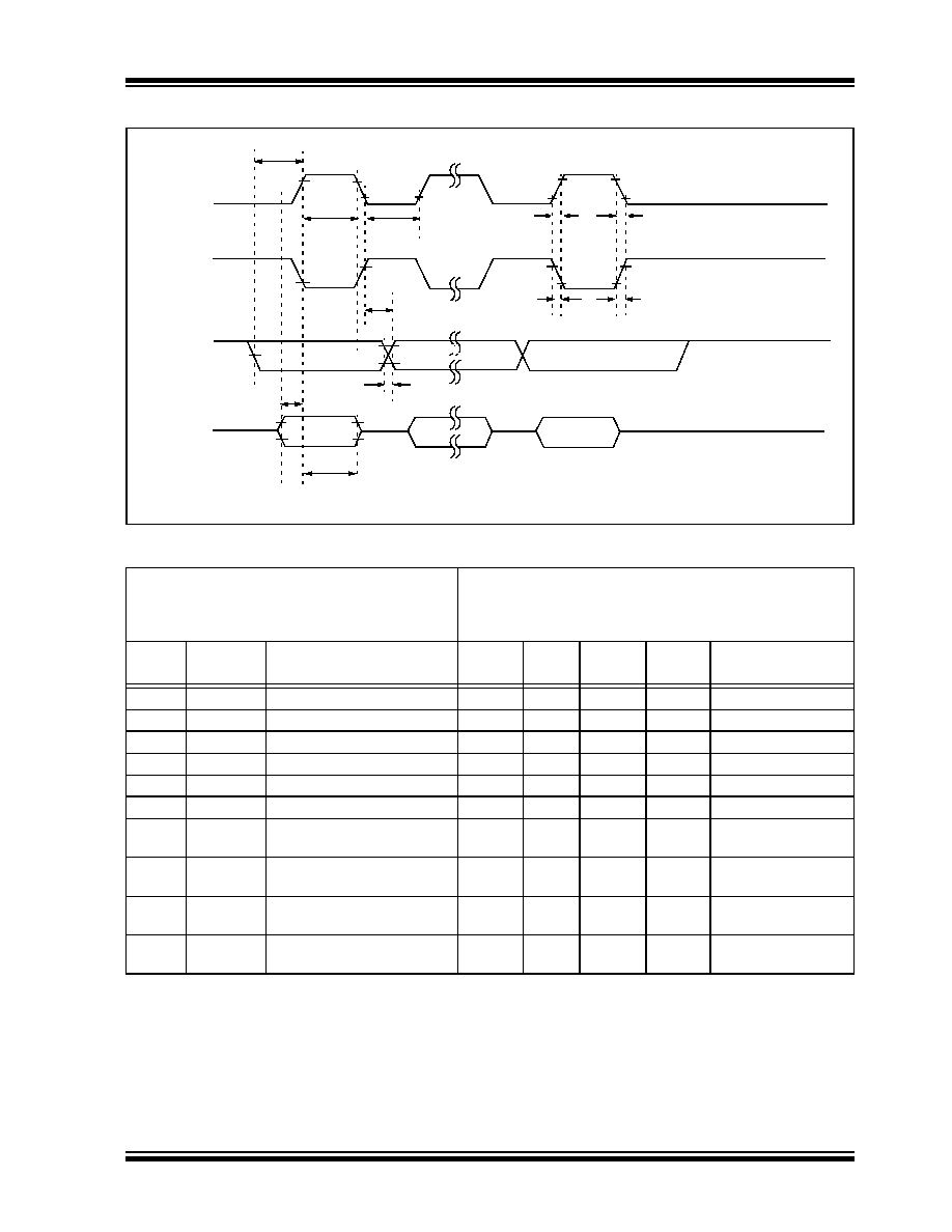
FIGURE 21-13:
SPI MODULE MASTER MODE (CKE =1) TIMING CHARACTERISTICS
TABLE 21-28: SPI MODULE MASTER MODE (CKE = 1) TIMING REQUIREMENTS
AC CHARACTERISTICS
Standard Operating Conditions: 3.3V and 5.0V (±10%)
(unless otherwise stated)
Operating temperature
-40°C
≤ TA ≤ +85°C for Industrial
-40°C
≤ TA ≤ +125°C for Extended
Param
No.
Symbol
Characteristic(1)
Min
Typ(2)
Max
Units
Conditions
SP10
TscL
SCKX output low time(3)
TCY / 2
—
ns
—
SP11
TscH
SCKX output high time(3)
TCY / 2
—
ns
—
SP20
TscF
SCKX output fall time(4)
—
ns
See parameter D032
SP21
TscR
SCKX output rise time(4)
—
ns
See parameter D031
SP30
TdoF
SDOX data output fall time(4)
—
ns
See parameter D032
SP31
TdoR
SDOX data output rise time(4)
—
ns
See parameter D031
SP35
TscH2doV,
TscL2doV
SDOX data output valid after
SCKX edge
—
30
ns
—
SP36
TdoV2sc,
TdoV2scL
SDOX data output setup to
first SCKX edge
30
—
ns
—
SP40
TdiV2scH,
TdiV2scL
Setup time of SDIX data input
to SCKX edge
20
—
ns
—
SP41
TscH2diL,
TscL2diL
Hold time of SDIX data input
to SCKX edge
20
—
ns
—
Note 1:
These parameters are characterized but not tested in manufacturing.
2:
Data in “Typ” column is at 5V, 25°C unless otherwise stated. Parameters are for design guidance only and
are not tested.
3:
The minimum clock period for SCK is 100 ns. Therefore, the clock generated in Master mode must not
violate this specification.
4:
Assumes 50 pF load on all SPI pins.
SCKX
(CKP = 0)
SCKX
(CKP = 1)
SDOX
SDIX
SP36
SP30,SP31
SP35
MSb
MSb IN
BIT14 - - - - - -1
LSb IN
BIT14 - - - -1
LSb
Note: Refer to Figure 21-1 for load conditions.
SP11
SP10
SP20
SP21
SP20
SP40
SP41
发布紧急采购,3分钟左右您将得到回复。
相关PDF资料
PIC16CR76T-I/SO
IC PIC MCU 8KX14 28SOIC
PIC18LF24K22-I/MV
IC PIC MCU 16KB FLASH 28UQFN
PIC18LF24K22-I/ML
IC PIC MCU 16KB FLASH 28QFN
PIC16CR76T-I/ML
IC PIC MCU 8KX14 28QFN
PIC16F627-04/P
IC MCU FLASH 1KX14 COMP 18DIP
PIC18F45J10-I/ML
IC PIC MCU FLASH 16KX16 44QFN
PIC18F24K22-I/ML
IC PIC MCU 16KB FLASH 28QFN
PIC16CR76-I/SS
IC PIC MCU 8KX14 28SSOP
相关代理商/技术参数
PIC18F13K50-I/P
制造商:Microchip Technology Inc 功能描述:20 Pin 8 KB Flash 512 RAM 15 I/O 10
PIC18F13K50-I/SO
功能描述:8位微控制器 -MCU 8KB Flash 512 RAM 15 I/O 10-B ADC USB 2.0 RoHS:否 制造商:Silicon Labs 核心:8051 处理器系列:C8051F39x 数据总线宽度:8 bit 最大时钟频率:50 MHz 程序存储器大小:16 KB 数据 RAM 大小:1 KB 片上 ADC:Yes 工作电源电压:1.8 V to 3.6 V 工作温度范围:- 40 C to + 105 C 封装 / 箱体:QFN-20 安装风格:SMD/SMT
PIC18F13K50-I/SO
制造商:Microchip Technology Inc 功能描述:20 Pin 8 KB Flash 512 RAM 15 I/O 10
PIC18F13K50-I/SS
功能描述:8位微控制器 -MCU 8KB Flash 512 RAM 15 I/O 10-B ADC USB 2.0 RoHS:否 制造商:Silicon Labs 核心:8051 处理器系列:C8051F39x 数据总线宽度:8 bit 最大时钟频率:50 MHz 程序存储器大小:16 KB 数据 RAM 大小:1 KB 片上 ADC:Yes 工作电源电压:1.8 V to 3.6 V 工作温度范围:- 40 C to + 105 C 封装 / 箱体:QFN-20 安装风格:SMD/SMT
PIC18F13K50-I/SS
制造商:Microchip Technology Inc 功能描述:8-Bit Microcontroller IC
PIC18F13K50T-I/SO
功能描述:8位微控制器 -MCU 8KB Flash 512 RAM 15 I/O 10-B ADC USB 2.0 RoHS:否 制造商:Silicon Labs 核心:8051 处理器系列:C8051F39x 数据总线宽度:8 bit 最大时钟频率:50 MHz 程序存储器大小:16 KB 数据 RAM 大小:1 KB 片上 ADC:Yes 工作电源电压:1.8 V to 3.6 V 工作温度范围:- 40 C to + 105 C 封装 / 箱体:QFN-20 安装风格:SMD/SMT
PIC18F13K50T-I/SS
功能描述:8位微控制器 -MCU 8KB Flash 512 RAM 15 I/O 10-B ADC USB 2.0 RoHS:否 制造商:Silicon Labs 核心:8051 处理器系列:C8051F39x 数据总线宽度:8 bit 最大时钟频率:50 MHz 程序存储器大小:16 KB 数据 RAM 大小:1 KB 片上 ADC:Yes 工作电源电压:1.8 V to 3.6 V 工作温度范围:- 40 C to + 105 C 封装 / 箱体:QFN-20 安装风格:SMD/SMT
PIC18F14K22-E/ML
功能描述:8位微控制器 -MCU 16KBFlash 512byteRAM 256bytesEEPROM
RoHS:否 制造商:Silicon Labs 核心:8051 处理器系列:C8051F39x 数据总线宽度:8 bit 最大时钟频率:50 MHz 程序存储器大小:16 KB 数据 RAM 大小:1 KB 片上 ADC:Yes 工作电源电压:1.8 V to 3.6 V 工作温度范围:- 40 C to + 105 C 封装 / 箱体:QFN-20 安装风格:SMD/SMT